● 4 YAMAHA High-speed SMT Lines
● 6 million daily SMT placements capability
● 400,000 daily DIP placements capability
● 500×600 mm Maximum Board Size
● 0.25"x 0.25" Minimum Board Size
● 450 mm Max. Width for Wave-Solder
● Passives Components Down to 0201 Size BGA and VFBGA Leadless Chip Carrier/CSP Double-Sided SMT Assembly Fine Pitch to 08 Mil BGA Repair and ReballPart Removal and Replacement
SMT and DIP/X-RAY Inspection/AOI Testing/In-circuit-test (ICT)/Flying Probe/Function Test/Burn-in/Finished products assembly

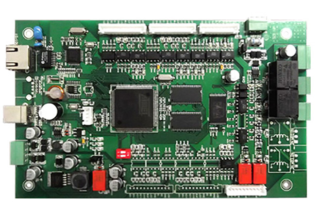
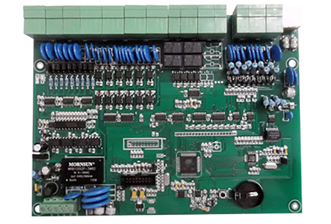
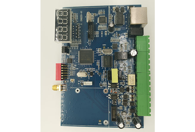
PCB assembly service
You need to only contact one company when you have PCB assembly requirements and it is CTT. PCB assembly price should not be your concern. Check below of our high quality PCB assembly services:
• One-stop manufacturing and assembly: a one-stop solutions for all your needs.
• A variety of PCB assembly services: SMT, THT, DIP, hybrid components, package (POP)
• Flexible batch assembly alternatives: prototype, small volume, high volume
• Parts sourcing: with 18 years of experience, we have a stable relationship with authorized electronic component manufacturers and distributors. We can get good price materials and our in house QC department do all inspection.
• Comprehensive quality assurance: From components to finished PCBA, from visual inspection to AOI and X-ray inspection, each step we have strict regulations to make sure all procedures is correct.
• Professional engineering team: We are highly qualified and committed to the success of your project. Price, quality and delivery are our commitment to your order.
PCB assembly equipment in CTT
1. There are four of the world's most advanced Yamaha SMT automatic patch lines. Its processing capacity is up to 4 million points per day.
2. 2 welding lines, 2 automatic production lines, up to 400,000 DIP plug-ins per day.
3. DIP capacity: Two welding lines, three assembly lines, one test line, one components solder shop, one maintenance line. In addition, we have BGA placement professional technology and rework technology.
Please check our PCB assembly service capabilities as below showing:
| Feature | Capability |
| Quality Grade | Standard IPC 2 |
| Number of Layers | 2 - 48layers |
| Build Time | 2days - 5weeks |
| Min Drilling Hole Diameter | 6mil, 4mil-laser drill |
| Min Width of Slot Hole (PTH) | 0.6mm |
| PTH Hole Size Tolerance | ±.003" (±0.08mm) - ±4mil |
| Material | FR-4, MCPCB, copper PCB、ROGERS、ARLON、Teflon、Composite PCB |
| Board Size | Max 500mm x 600mm |
| Board Thickness | 0.25mm - 5mm |
| Copper Weight | 0.5oz - 6.0oz |
| Inner Layer Copper Weight | 0.5oz - 6.0oz |
| Min Tracing/Spacing | 3mil/3mil |
| Solder Mask Color | Green, White, Blue, Black, Red, Yellow |
| Silkscreen Color | White, Blue, Black, Red, Yellow |
| Surface Finish | HASL - Hot Air Solder Leveling |
| Lead Free HASL - RoHS | |
| ENIG - Electroless Nickle/Immersion Gold - RoHS | |
| ENEPIG - Electroless Nickel Electroless Palladium Immersion Gold - RoHS | |
| Immersion Silver - RoHS | |
| Immersion Tin - RoHS | |
| OSP -Organic Solderability Preservatives - RoHS | |
| Min Annular Ring | 3mil |
| SM Tolerance (LPI) | .003" (0.075mm) |
| Test | E test, flying probe or testing fixture |
| Impedance tolerance | ±5% - ±10% |
| SMD Pitch | 0.2mm(8mil) |
| BGA Pitch | 0.2mm(8mil) |
| Chamfer of Gold Fingers | 20, 30, 45, 60 |
| Other Techniques | Gold fingers |
| Blind and Buried Holes | |
| peelable solder mask | |
| Edge plating | |
| Carbon Mask | |
| Kapton tape | |
| Countersink/counterbore hole | |
| Half-cut/Castellated hole | |
| Press fit hole | |
| Via tented/covered with resin | |
| Via plugged/filled with resin | |
| Via in pad | |
| Electrical Test |
Learn more about PCB assembly service NOW? Click your favorite button in the right side and contact us.