● 4 YAMAHA High-speed SMT Lines
● 6 million daily SMT placements capability
● 400,000 daily DIP placements capability
● 500×600 mm Maximum Board Size
● 0.25"x 0.25" Minimum Board Size
● 450 mm Max. Width for Wave-Solder
● Passives Components Down to 0201 Size BGA and VFBGA Leadless Chip Carrier/CSP Double-Sided SMT Assembly Fine Pitch to 08 Mil BGA Repair and ReballPart Removal and Replacement
SMT and DIP/X-RAY Inspection/AOI Testing/In-circuit-test (ICT)/Flying Probe/Function Test/Burn-in/Finished products assembly


As a manufacturer of PCB and PCBA, how do we control the quality of PCB and PCBA assembly production?
1. PCB circuit board manufacturing: after receiving the PCBA order, analyze the Gerber file, pay attention to the hole spacing of the printed circuit board and the bearing capacity of the PCB board.
2. Purchasing and inspection of components: Material purchasing must from regular company or original factories. In addition, special inspection positions are set up to make sure components are all in good quality.
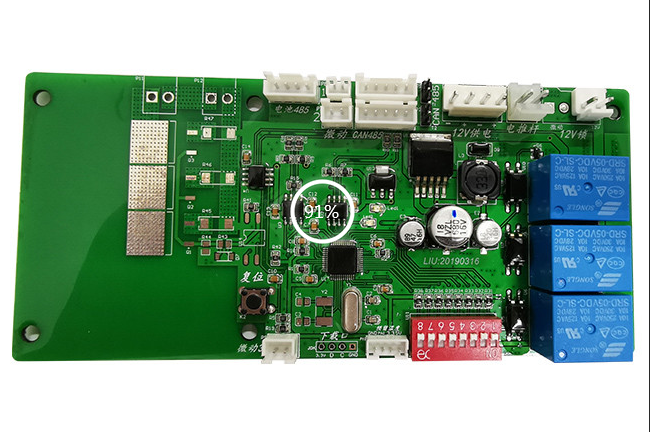
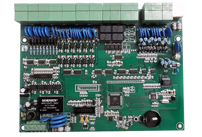
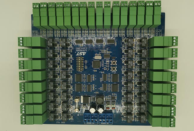
3. SMT processing
Solder paste printing and reflow oven temperature control are key points. In addition, AOI testing needs to be strictly implemented to minimize the adverse effects caused by human factors.
4. DIP plug-in processing
In the plug-in process, the mold design for over-wave soldering is a key point. How to use the mold maximize the probability of providing good quality after the furnace? As a electric product assembly manufacturer, our PE engineers have great experience in it.
5. Firing program
As a experienced pcb assembly factory, we usually advise customers to set up some Test Points on the PCB in order to test the PCB and the PCBA circuit continuity after soldering all components.
6. PCB board test
For orders with PCBA test requirements, the main test contents include ICT (In Circuit Test), FCT (Function Test), Burn In Test (aging test), temperature and etc.. According to the customer's test plan. We provide the report data.
We are a perfect China PCB factory and an experienced pcb assembly processing manufacturer!
PCB processing capability
| PCB service | Process capability |
| Layer | 1-20 layers |
| Maximum size | ≤600*500mm |
| Thickness | 0.1-5.0mm |
| Wire copper foil thickness | 17-343um(10oz) |
| Minimum linewidth / line distance | 0.075/0.065mm(3mil/2.8mil) |
| Minimum aperture | 0.15mm(6mil) |
| Minimum welding pad | 0.2mm(8mil) |
| Impedance control | +/-10% |
| Shape processing accuracy | +/-0.10mm(4mil) |
| Board type | FR-4, aluminum - base, copper -base, ROGERS, ARLON, Teflon, composite |
| Surface treatment | Tin spray, ENIG, Immerse Au, immersion silver, im mersion tin, osp, gold osp, electrospray tin |
PCB ASSEMBLY CAPABILITY
| SMT service | Process capability |
| Processing type | SMT, DIP, After welding, test |
| Maximum board | L50×W50mm~L510×W460mm |
| Maximum thickness | 3mm |
| Minimum thickness | 0.5mm |
| Minimum component | 1005 |
| Maximum component size | 150mm*150mm |
| Minimum pin component spacing | 0.3mm |
| Minimum bga spacing | 0.3mm |
| Maximum component mounting accuracy(100FP) | Whole assembly accuracy up to ±50 micron,whole process repetition accuracy ±30 micron. |
| SMT capacity | 4 million pins / day |
| DIP capacity | 100 thousand/ day |