● 4 YAMAHA High-speed SMT Lines
● 6 million daily SMT placements capability
● 400,000 daily DIP placements capability
● 500×600 mm Maximum Board Size
● 0.25"x 0.25" Minimum Board Size
● 450 mm Max. Width for Wave-Solder
● Passives Components Down to 0201 Size BGA and VFBGA Leadless Chip Carrier/CSP Double-Sided SMT Assembly Fine Pitch to 08 Mil BGA Repair and ReballPart Removal and Replacement
SMT and DIP/X-RAY Inspection/AOI Testing/In-circuit-test (ICT)/Flying Probe/Function Test/Burn-in/Finished products assembly


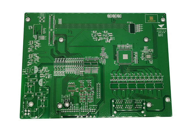
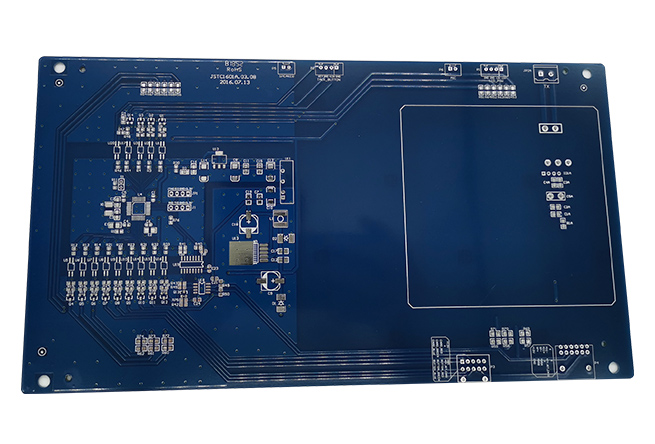
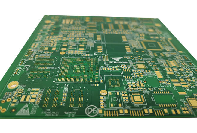
What is a high frequency (HF) PCB?
Electronic devices with high frequency is the developing tendency nowadays, especially in wireless network. Satellite communications are developing rapidly, and information products are moving towards high speeds and high frequency. Accordingly, developing new products always requires high-frequency substrates. These communication products, like satellite systems, mobile phones, must use high-frequency PCBs.
The characteristics of high frequency PCB.
1. DK should be small and stable enough, usually as small as possible. Because high DK may cause signal transmission delays.
2. DF should be small, which mainly affects the quality of signal transmission, and smaller DF can reduce signal loss accordingly.
3. In a humid environment, the water absorption rate must be low. Otherwise it will affect DK and DF.
4. It must be good for the heat resistance, chemical resistance, impact resistance, and peel resistance.
It has special materials requirements for the high frequency boards for wireless applications and data rates in the high GHz range:
1. Adapted dielectric constant.
2. Low attenuation, effective signal transmission.
3. Uniform structure, low insulation thickness and dielectric constant tolerance.
In general, the high frequency can be defined as a frequency above 1 GHz. Currently, PTFE materials are widely used in high-frequency PCB manufacturing, also known as Teflon, and their frequencies are usually higher than 5 GHz. In addition, FR4 or PPO substrates can be used for product frequencies between 1 GHz and 10 GHz.
Check our HF PCB capabilities by reviewing below table:
| Feature | Capability |
| Quality Grade | Standard IPC 2 |
| Number of Layers | 2 - 20layers |
| Build Time | 2days - 5weeks |
| Material | RO4003C, RO4350B, Ro3003, Ro3010, RT5880 etc. |
| Board Thickness | 0.25mm - 5.0mm |
| Copper Weight(Finished) | 0.5oz - 2.oz |
| Min Tracing/Spacing | 3mil/3mil |
| Solder Mask Sides | As per the file |
| Solder Mask Color | Green, White, Blue, Black, Red, Yellow |
| Silkscreen Sides | As per the file |
| Silkscreen Color | White, Black, Yellow |
| Surface Finish | Electroless nickel/immersion gold (ENIG) - RoHS |
| Immersion silver - RoHS | |
| Immersion tin - RoHS | |
| Organic solderability preservatives - RoHS | |
| Min Annular Ring | 4mil |
| Min Drilling Hole Diameter | 6mil |
| Impedance tolerance | ±10% |
| Other Techniques | Peelable solder mask |
| Gold fingers | |
| Carbon oil | |
| Countersink holes |
Let’s start to discuss your HF board today? Just click your favorite button in the right side.