1) Place of Origin: Shenzhen, China
2) Base Material: FR4
3) Copper Thickness: 32um
4) Board Thickness: 1.8mm
5) Min. Hole Size: 0.15mm
6) Min. Line Width: 0.1mm
7) Min. Line Spacing: 0.1mm
8) Surface Finishing: lead free hasl
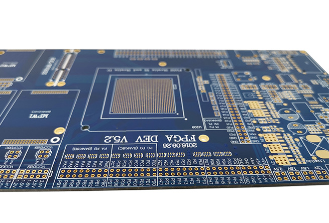
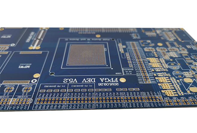
9) Solder mask: Blue
10) Board Thickness Tolerance: ±10%
11) Service: PCB&PCBA
13) E-test: 100%
All multilayer boards are printed with 36t screen, the resistance welding oil is 50 tons thicker than the traditional 43t, which provides reliability guarantee for the bga and more precise fine lines.