Place of Origin: Guangdong, China (Mainland)
Brand Name: HKCT TECH OEM PCB
Model Number: FR-4 TG130/150/170 multi pcb
Base Material: Fr-4 TG130/150/170
Copper Thickness: 1oz-2oz
Board Thickness: 7mm
Min. Hole Size: 0.15mm, 0.20mm
Surface Finishing: HASL,LEAD FREE HASL,OSP
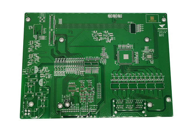
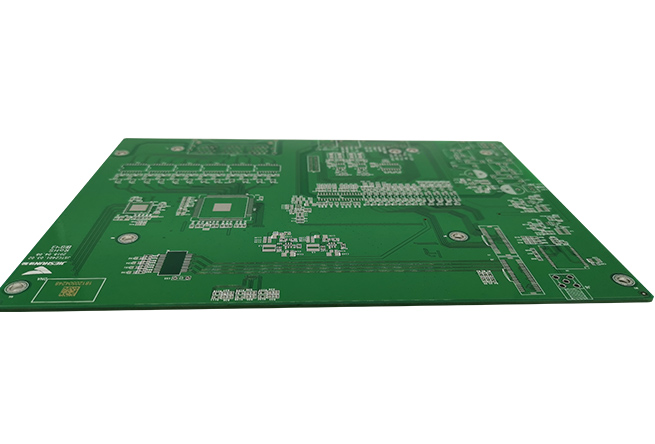
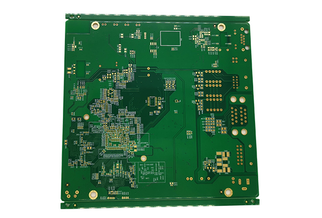
Product name: Factory price high TG Fr4 Metal Alu Small Printed Circuit Board
PCB type: Electronics Manufacturing
Number of Layer: Double Layer PCB,Multilayer PCB
Certification of quantum board led: ISO,SGS,ISO,ROHS
Testing service: Omron AOI/X-Ray/ICT/Solder Paste Testing/Function Testing
Service: PCBA,PCB&PCBA Design&Clone&Production
Application: Consumer Electronics,Industrial,Electronical Products,Battery Pack
PCB Assembly service: SMT THT DIP


PCB fabrication FAQ:
Have you met poor solderability issues in your pcb?
Poor solderability is one of the serious problems for printed circuit board, especially for batch pcb problems. The possible reasons include a lot, such as surface contamination, oxidation, black nickel, nickel thickness abnormality, solder-proof SCUM (shadow), long storage time and etc.
Pollution problem can be solved easily, Other problems are more troublesome, and there is no way to find out through the inspection of the feed. So it is very necessary to pay attention to the process capability and quality control plan of the PCB manufacturers. For example, black nickel, it needs to pay attention to see whether the PCB factory is sufficient in frequency of analysis of its own gold line syrup, whether the concentration is stable, whether a regular stripping test and a phosphorus content test are set to detect by the pcb supplier and so on. If all can be done well, the issue possibility of a pcb batch is very small.
The PCB manufacturing process is a very rigorous and technically process. Any manufacturer neglect any detail that can cause fatal problems to PCB quality. Please carefully choose your PCB manufacturing partner.
PCB processing capability
| PCB service | Process capability |
| Layer | 1-20 layers |
| Maximum size | ≤600*500mm |
| Thickness | 0.1-5.0mm |
| Wire copper foil thickness | 17-343um(10oz) |
| Minimum linewidth / line distance | 0.075/0.065mm(3mil/2.8mil) |
| Minimum aperture | 0.15mm(6mil) |
| Minimum welding pad | 0.2mm(8mil) |
| Impedance control | +/-10% |
| Shape processing accuracy | +/-0.10mm(4mil) |
| Board type | FR-4, aluminum - base, copper -base, ROGERS, ARLON, Teflon, composite |
| Surface treatment | Tin spray, ENIG, Immerse Au, immersion silver, im mersion tin, osp, gold osp, electrospray tin |
PCB ASSEMBLY CAPABILITY
| SMT service | Process capability |
| Processing type | SMT, DIP, After welding, test |
| Maximum board | L50×W50mm~L510×W460mm |
| Maximum thickness | 3mm |
| Minimum thickness | 0.5mm |
| Minimum component | 1005 |
| Maximum component size | 150mm*150mm |
| Minimum pin component spacing | 0.3mm |
| Minimum bga spacing | 0.3mm |
| Maximum component mounting accuracy(100FP) | Whole assembly accuracy up to ±50 micron,whole process repetition accuracy ±30 micron. |
| SMT capacity | 4 million pins / day |
| DIP capacity | 100 thousand/ day |